The minister stated that the country is steadily moving towards its 10-year target of training 85,000 engineers in semiconductor design.
Vaishnaw said world-class Electronic Design Automation (EDA) tools supported by companies such as Synopsys, Cadence Design Systems, Siemens, Renesas Electronics, Ansys and AMD have been made available in 315 academic institutions across the country.
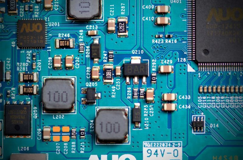
With access to these advanced tools, students are gaining practical experience in designing semiconductor chips.
The chips designed by students are being fabricated and tested at the Semiconductor Laboratory (SCL) in Mohali, providing hands-on exposure to the entire semiconductor value chain — from design and fabrication to packaging and testing.
According to the minister, the initiative has evolved into the world’s largest open-access EDA programme, with more than 1.85 crore hours of EDA tool usage recorded for chip design training so far, and the figure continues to rise.
Vaishnaw added that students from academic institutions across the country — from Assam to Gujarat and from Kashmir to Kanyakumari — are now actively participating in semiconductor design, marking a significant milestone in India’s push for technological capability and self-reliance.
Highlighting global industry demand, the minister said that as the semiconductor industry expands from its current size of USD 800–900 billion to nearly USD 2 trillion, there will be a need for around two million skilled professionals worldwide. This presents significant employment opportunities for India’s youth.
Vaishnaw further announced that under India Semiconductor Mission 2.0, the programme will be expanded from 315 to 500 academic institutions.
The expansion aims to build a strong and continuous talent pipeline in semiconductor design, fabrication, packaging and testing across every state in the country.
Reiterating the government’s commitment, Vaishnaw said India is working to build a robust and self-reliant semiconductor ecosystem. Through talent development, infrastructure creation and industry collaboration under India Semiconductor Mission 2.0, the country aims to establish itself as a global semiconductor hub.